Photonic Detectors
Contact usX-RAY integrated circuits for direct and indirect photon sensing detectors
X-RAY photon sensing panels make use of the same amorphous silicon (aSi) substrate as the one used in TFT-LCD technologies for indirect sensing while the direct sensing uses the same crystal silicon (Si) as standard CMOS integrated circuits and by analogy to LCD micro-displays. The fundamental difference is in the functionality where the LCD panels are emitting visible light through the TFT pixels while the X-RAY panels are absorbing X-Ray photons through the TFT pixels. The control and detection of the number of photons absorbed in each pixel is one of the main function of our X-RAY chipset.
Indirect X-RAY photon sensing
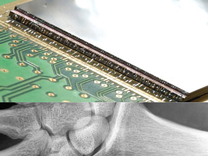
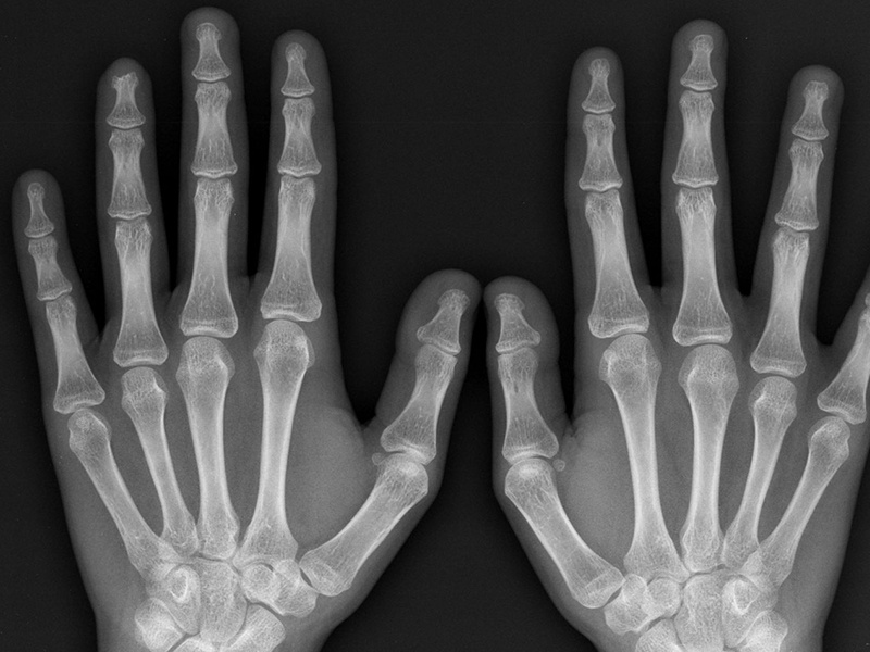
The typical structure of an Indirect X-RAY panel is a stacking of a scintillator film layered on top of the TFT panel where a matrix of photodiodes is patterned pixel by pixel with the aSi transistors. The incoming X-RAY photons are converted into light by the scintillator and guided to the photodiodes of each pixel inside of which the light is converted and stored as electrical charges. Thus, these charges are available to the extraction through the TFT transistor. Our family of X-Ray integrated circuits specializes in controlling the scan and transfer of the electrical charges stored in each photodiode pixel. This is enabled by our 3 levels TFT gate drivers and our digital Read Out Integrated Circuit (ROIC). The gate drivers function is to scan sequentially and line by line the switching of the TFT devices of the active matrix, while the ROICs integrate in parallel the stored charges of all columns for each line. Our gate drivers offer a diversity of scanning options among which all ON for reset operation, line scan grouping, left-right scan and high speed data loading. Our ROIC Analog Front End (AFE) allows a flexible integration time for static and dynamic applications and our proprietary ADC architecture enables 16-bit resolution.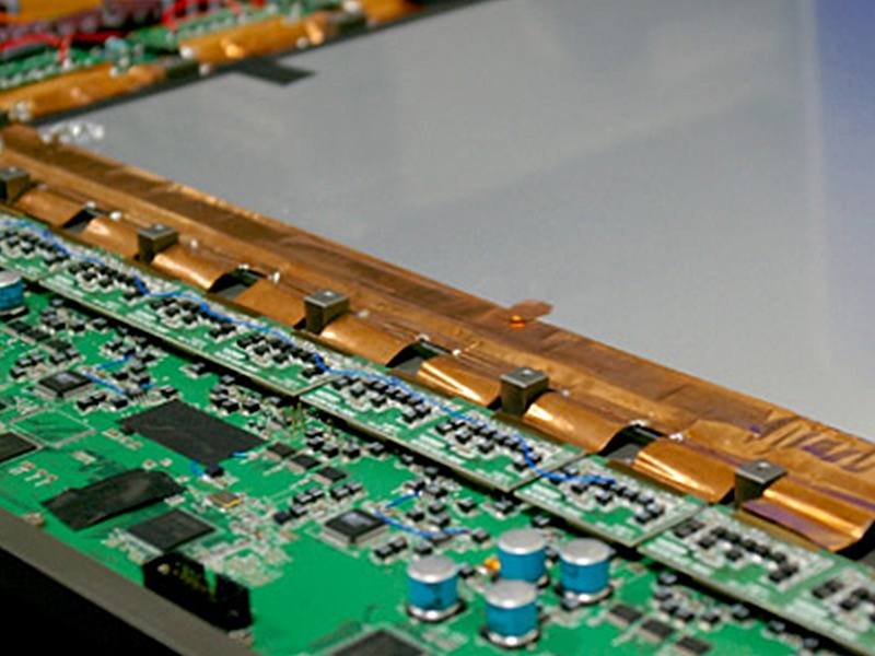
Indirect X-RAY photon sensing
The typical structure of an Indirect X-RAY panel is a stacking of a scintillator film layered on top of the TFT panel where a matrix of photodiodes is patterned pixel by pixel with the aSi transistors. The incoming X-RAY photons are converted into light by the scintillator and guided to the photodiodes of each pixel inside of which the light is converted and stored as electrical charges. Thus, these charges are available to the extraction through the TFT transistor. Our family of X-Ray integrated circuits specializes in controlling the scan and transfer of the electrical charges stored in each photodiode pixel. This is enabled by our 3 levels TFT gate drivers and our digital Read Out Integrated Circuit (ROIC). The gate drivers function is to scan sequentially and line by line the switching of the TFT devices of the active matrix, while the ROICs integrate in parallel the stored charges of all columns for each line. Our gate drivers offer a diversity of scanning options among which all ON for reset operation, line scan grouping, left-right scan and high speed data loading. Our ROIC Analog Front End (AFE) allows a flexible integration time for static and dynamic applications and our proprietary ADC architecture enables 16-bit resolution.